- Silicon detectors
- Radiation hardness & radiation effects
- Characterization methodologies
Passionate of science since high school, I graduated in 2016 at the University of Milan with a thesis on the characterization of CMOS detectors. I joined STREAM in September 2017 and I hold a PhD studentship from University of Geneva.
My studies in STREAM are focused on high voltage CMOS detectors for the ATLAS upgrade.
I collaborate in the STREAM Work Package 4: Validation and Qualification.
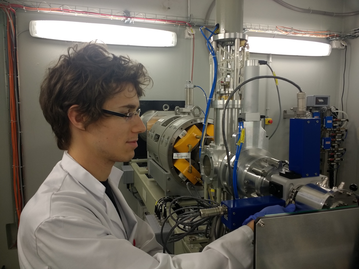
The objective of the laboratory measurements is to determine the characteristics of the sensitive part of the CMOS detectors, in particular the depth of the depletion region, and to get information about the type of charge collection in different positions inside the sensor. To achieve this goal, a laser is used to generate charge in a very precise position inside the detector and the resulting signal is amplified and measured. This experimental technique is called TCT (Transient Current technique). These measurements are being carried out on unirradiated and irradiated chips to verify the variation of the parameters of interest with the dose. Similar measurements on different sensors have been carried out during his first secondment at the University of in Liverpool.
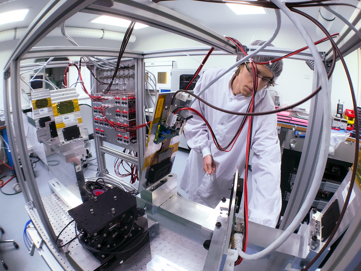
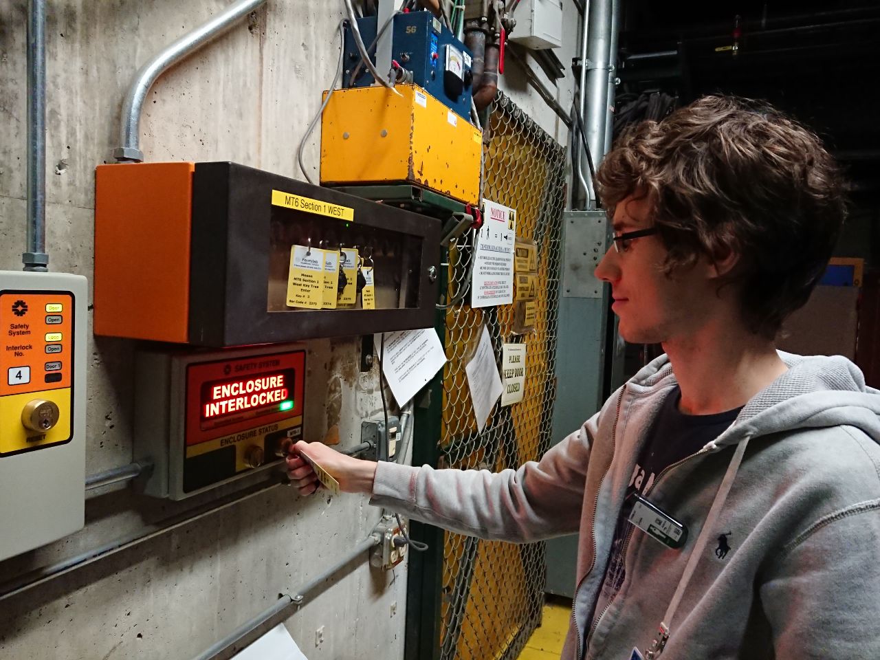
The aim of test- beams is to evaluate the performance of the detector prototypes in a real data-taking environment. The detectors under study are placed in a beamline and hit with high energy particles (typically charged pions). An external telescope composed of an array of various silicon pixel detectors is used to reconstruct the tracks. The efficiency of the HV-CMOS detector is then measured by comparing the number of reconstructed tracks crossing the sensor with the number of recorded hits. Other parameters have been also studied, as the dependency of clusters size (i.e. the number of pixels turned on by a single particle) with the substrate resistivity and the bias voltage. Furthermore, I also contribute to the upgrade of the experimental setup for the 2018 measurement campaign at the Fermilab National Laboratory (FNAL).
The simulation of the digital part of a detector is crucial to find possible inefficiencies before producing the sensors. To do so I use samples simulated with the official ATLAS software framework (to accurately reproduce the conditions expected a the HL-LHC) to extract all the information needed (e.g. which pixels have been turned on at each event and how much charge has been generated in them). These data are available to all the groups studying the digital CMOS architecture, in order to have a unique and common starting point to compare the different logic implementations.
Secondments
|
Host Institution and Secondment Topic |
Expected secondment period |
|
Liverpool (UK), Characterization of LFoundry sensors |
2 weeks in June 2017 |
|
University of Milan (IT), X-ray irradiation, first test of module flex |
4 weeks in October 2017 |
|
University of Milan (IT), Module assembly and flex design |
3weeks in April-Mai 2018 |
My research is contributing to assess the suitability of HV-CMOS detectors for high-energy physics applications at LHC, in particular by studying their radiation hardness and performances. I have also contributed with improvements in the experimental techniques used to characterize silicon detectors. Furthermore, I have the possibility to collaborate with different groups outside my university (Bern, Liverpool, CERN, etc.), to learn new languages and to create a network to rely on.
Thanks to MSC fellowship and its complete training program, I have increased my knowledge in the technical fields, in complementary skills and in management. This will be a great value in a future search for a job.