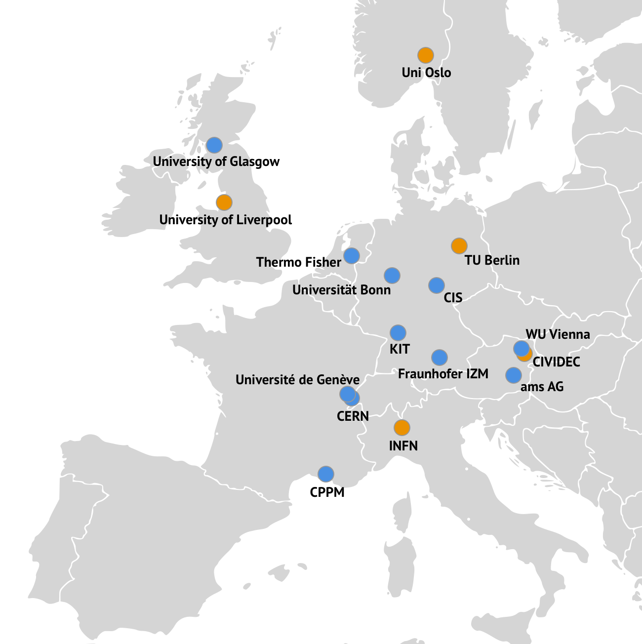
Our Beneficiaries
Scientific Network Coordinator: Dr Heinz Pernegger , Dr Mar Capeans
CERN is responsible of the Work Package 1- Project Management (H. Pernegger), Work Package 7- Training (M. Capeans) and, together with University of Geneva, of the Work Package 4 - Validation and Qualification
Work pachage 1 is lead by Dr. Heinz Pernegger (CERN). Heinz is a CERN Senior Physicist and correctly co-leads the development of novel CMOS sensors as tracking detectors for the ATLAS experiment at CERN’s Large Hardon Collider. The has received his PhD from the Technical University Vienna in 1996, spent years of post-doctoral studies at Bookhaven National Laboratory and Massachusetts Institute of Technology. Since 2000 his research focuses at the development and construction of novel silicon detector systems for experiments at CERN.
Work Package 4 is co-led by Dr Petra Riedler (CERN) and Dr. Heinz Pernegger (CERN). It focuses on validation and qualification of sensors in laboratory, irradiations campaigns and test beams. The stringent requirements for next-generation imaging and tracking sensors will need to be optimized for spatial resolution, charge collection efficiency, fast signal response and operational stability. Device simulation will further optimize the pixel designs for maximum sensitivity. Projects in WP4 evaluate the different CMOS sensors with readout electronics for monolithic and hybrid implementations and assess their performance towards user specifications of WP2. The direct feedback into the technology studies in WP2 and designs in WP3 will allow to fully explore the technological advantages of CMOS and to optimize smart sensors to application specific requirements.
Dr Mar Capeans (CERN) is leading the Work Package 7- Training. STREAM focuses on bringing top-level training and education to each researcher in the network. The training provided focuses on scientific, technological and complementary skills for individual and as teams. Trainings are organised as individual courses selected by the ESRs and academic supervisors or network wide training common to all the ESRs.
Dr Prof. Peter Keinz from WU Wien is the responsible of the Work Package 6 - Technology Valorisation.
Potential fields of application will be systematically identified and evaluated, feasible commercialization strategies will be crafted. WP6 is therefore the framework where wide knowledge-sharing of the research to industry and academia inside and outside the project happens. STREAM partner WU-Wien, leading university in the field of Open and User Innovation Management, leads the development of business cases for different applications and provide business training for STREAM ESRs. The process is assisted by the CERN member states industry liaison officers, technology transfer officer networks, and the ATLAS technology transfer offices ATLAB. Projects in WP6 foster entrepreneurial skills and knowledge.
Dr Luigi Mele , as Scientist in Charge from Thermo Fisher Scientific (ex FEI) is responsible for the Work Package 5 - Technology Integration
Luigi Mele received his Phd at University of Naples Federico II in 2004 for a work on lifetime tailoring techniques to improve the reverse recovery of power diodes. Next, he moved to Delft University of Technology to develop MEMS-based chips for in-situ electron microscopy. Since 2011 he is scientist at FEI Company (now Thermo Fisher Scientific).
The Work Package 5 focuses on the integration of CMOS sensors to functional modules for applications in the ATLAS ITK as well as for feasibility tests in electron microscopy, led by FEI, and multi-functional environmental sensors, led by CiS. Prototype sensors of WP4 will be integrated with existing powering and readout systems. “Demonstrator” modules will serve as realistic integration of sensors and FrontEnd electronics. Novel packaging technologies using 3D integration, through-silicon vias7 and redistribution layers, developed by IZM and CiS, are exploited for integration to hybrid pixel detectors which combined analogue functionality in the sensor with digital processing in separate ASICs. The functional integrated sensor modules will be tested against the specifications needed for various applications. Projects in WP5 are application specific and target developments for detector systems at CERN and prototype modules for STREAM industrial applications where radiation hardness, fast signal processing and low-cost manufacturing are of prime importance.
http://www.cppm.in2p3.fr/sommaire.php3?lang=en
Dr Prof Marlon Barbero and Alexandre Rozanov are the Scientists in Charge for the STREAM Work Package 2- CMOS Technologies Assessment.
The WP2 explores CMOS sensor technologies. CMOS processes are industrially available in a large variety and can provide high-performance sensors at reduced costs. Among them are HV/HR-CMOS and imaging processes featuring high breakdown voltages and moderate to large depletion zones. These allow for the application of a voltage to rely on charge drift rather than diffusion, thereby enabling much higher radiation-hardness than present state-of-the-art monolithic active pixel sensors (MAPS) for imaging applications5. The enlarged depleted volume under deep n-wells allows the efficient detection of charge particles as well as enhanced X-rays and near-infrared (NIR) quantum detection efficiency (QDE).
Projects in WP2 tailor the sensor processing to requirements of large size future scientific instruments as well as cost-effective sensor components for industrial applications. The projects will also explore both Capacitive Coupled Pixel Detectors (CCPD) connected to digital readout chips as well as full Monolithic (MAPS) sensors. ESRs will participate in the design, tests and development of different CMOS technologies to improve their radiation hardness 10 to 100 fold over present CMOS sensors. A key focus of this WP will be the definition of sensor specifications to be used for different applications.
http://hep1.physik.uni-bonn.de/
Dr Prof Norbert Wermes, is the Scientist In Charge from Bonn University and he is responsible for the Work Package 3 - Smart Sensor Design and Layout.
The Work Package 3, focuses on the layout of smart sensors and full monolithic ICs in radiation-hard CMOS technologies. Radiation hardness is achieved through special layout techniques and biasing of the substrate to create an extended depleted zone. Charges generated in this zone will drift towards a deep n-well node, which acts as a charge collection electrode as shown in the figure above6. Due to the creation of a drift field under external bias, superior radiation hardness and faster signal response can be achieved. Solutions to harden monolithic sensor towards ionization damage will be investigated and implemented in demonstrator sensors. NMOS/PMOS circuitry allows first stage amplification and signal processing directly on the sensor, hence the implementation of “Smart” on-pixel signal processing. This principle has recently been demonstrated on early prototypes by STREAM partners AMS, FEI, uBonn, KIT and CNRS. AMS possesses various 0.35µm and 0.18µm CMOS and HV-CMOS processing technologies as well as a large experience on design and processing of optical sensors. AMS will focus on enhancing the radiation hardness of their technologies enabling AMS to penetrate new market segments: medical (X-ray detection), industrial and avionics applications (X-ray and NIR detection).
Prof. Ivan Peric is the Scientist in Charge for Karlsruhe Institute of Technology and collaborates in Work Package 5 - Technology Integration.
Prof. Craig Buttar is the Scientist in Charge for University of Glasgow and collaborate the Work Package 4 - Validation and Qualification.
http://www.unige.ch/international/index_en.html
Prof. Giuseppe Iacobucci and Dr S. Gonzalez Sevilla are the Scientists in Charge for University of Geneva and collaborate to the Work Package 4 - Validation and Qualification.
Dr Ingrid Jonak-Auer is the Scientist in Charge for ams AG. I.Jonak-Auer works at ams AG as Manager of the Photonic Devices Group. She’s specialized in process and device development for optical sensors as well as optical system simulations. She received her MSc in Physics and Mathematics from the University of Vienna and her PhD in Material Science from the University Leoben, Austria. Before joining ams AG she held positions as Research Assistant at the Clarendon Laboratory, University of Oxford, UK and as Software engineer at Siemens AG, Vienna, Austria.
The company ams AG contributes to the Work Package 3 - Smart Sensor Design and Layout (ESR#3) and to the Work Package 4 - Validation and Qualification (ESR#15).
http://www.cismst.org/en/profil/willkommen/
Ralf Roder the Scientists in Charge for CiS Forschungsinstitut für Mikrosensorik und Photovoltaik GmbH. CiS contributes to the Work Package 5 - Technology Integration.
Dr Thomas Ortlepp from CiS is also strongly contributing to the STREAM ITN as STREAM Supervisory Board chairperson.
Our Partners
Prof. Heidi Sandaker is the scientist in charge of University of Oslo.
Dr Gianluigi Casse is the scientist in charge of University of University of Liverpool.
Prof Tomislav Suligoj is the scientist in charge representing the University of Zagreb.