Hello! I am Roberto, I have studied electronics engineering at the University of Catania where I took my BSc and MSc in July 2013 and 2016 respectively. During the last year of my university studies, I came at CERN as a technical student working in the n_ToF experiment, where I worked on JAVA development, and I have designed, produced and tested some electronics for the upgrade of TAC detector (Total Absorption Calorimeter).
I was sixteen when I came visiting CERN with my school, and after ten years, in September 2016 I joined STREAM as a CERN fellow, and I am doing my PhD at the University of Oslo.
I love to work in a challenging environment and to experiment. I like to put myself all the time pursuing new goals, especially in fields that I have never explored before.
My mantra is "move and never stay steady". I love to explore the world and meet people from all over the world getting in touch with different cultures and lifestyles. I love my job because it allows me to do it when I work and even when I do not.
As Early Stage Researcher (ESR 9 WP4) in the STREAM ITN working at CERN and doing my PhD at the University of Oslo, I contribute to the development and test of novel pixel sensors, comprising laboratory measurements, irradiations campaigns and test beams. My particular contribution to the project is the design and validation of a large area monolithic pixel detector, which should meet the ATLAS inner tracker specifications, aiming to reduce the material budget and improve the overall performance.
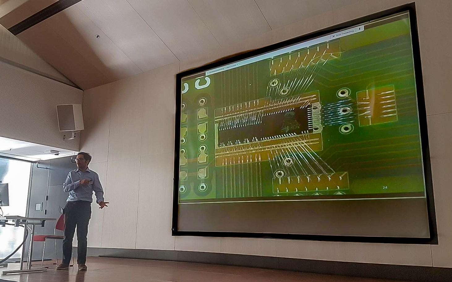
The first part of my work in the project has been directly related to the design of a monolithic pixel detector called MALTA (Monolithic pixel sensor from ALICE To ATLAS). My contribution to this chip is the design of an output buffer, which allows sending data from the pixel detector to the external world at high speed (5 Gbit per second) with low power consumption. The name of this circuit is LAPA (LVDS for Atlas Pixel Apparatus). The buffer design is directly related to the assembly of a large area pixel detector. Indeed, it has to match the data rate requirements of a module of four-pixel sensors. I have integrated the buffer into the MALTA chip and designed a test chip with ten input/output buffer channels to fully test its functionality.
Sequentially, I have started with the preparation and design of test cards for single chips as well as modules, in collaboration with the rest of the testing team. I am currently involved in the test of both MALTA and LAPA, with a particular focus on irradiation and test beam, for what concern the organisation and the actual tests.
The characterization of MALTA CMOS chip will allow me to investigate the possible connections to build a four-sensor module, minimizing the dead area of the full detector, which is one objective of the project.
Secondments
|
Host Institution and Secondment Topic |
Expected secondment period |
|
University of Oslo (NO), Science ethics course |
10 days in May 2017 |
|
University of Glasgow (UK), Design of testboard of LAPA chip for high-speed data transmission |
One week in July 2017 |
|
UniBonn (DE), Test beam measurement on MALTA |
One week in March 2018 |
| Univ. of Glasgow (UK), Test of LAPA chip for high-speed data transmission and MALTA | 10 days in June 2018 |
In the high energy physic experiment, a crucial aspect of the detectors is the material budget and the coverage of the full area of an event. The usage of novel interconnection technologies in combination with monolithic CMOS sensors would give a substantial contribution on the pursuit of improving this two aspects of the detectors, with an expected reduction of the cost.
The development of this technologies, driven by physics research, would allow increasing the possibility of discoveries. Moreover, creating more expertise and structures to develop such sensors would enable introducing their usage in consumer and medical applications, such as imaging and cameras, with improved performance and reduced costs.