HVCMOS sensors TCAD simulation
HVCMOS sensors characterization in harsh radiation environments


I was born and raised in China. I graduated from the Jiangnan University with a B.Sc. in Physics and then received an M.Sc. in Condensed Matter Physics from Beijing Normal University in 2014. I joined CPPM, Aix-Marseille University as a PhD student in 2016 through STREAM programme.
I collaborate in the STREAM Work Package 2. Specifically, I focus on testing prototypes developed by the CPPM laboratory and by other institutes in the STREAM collaboration. The objective of my work is to demonstrate how the changes to the design concept affect the goals pursued in terms of radiation hardness, increased breakdown voltage and overall architecture performances.
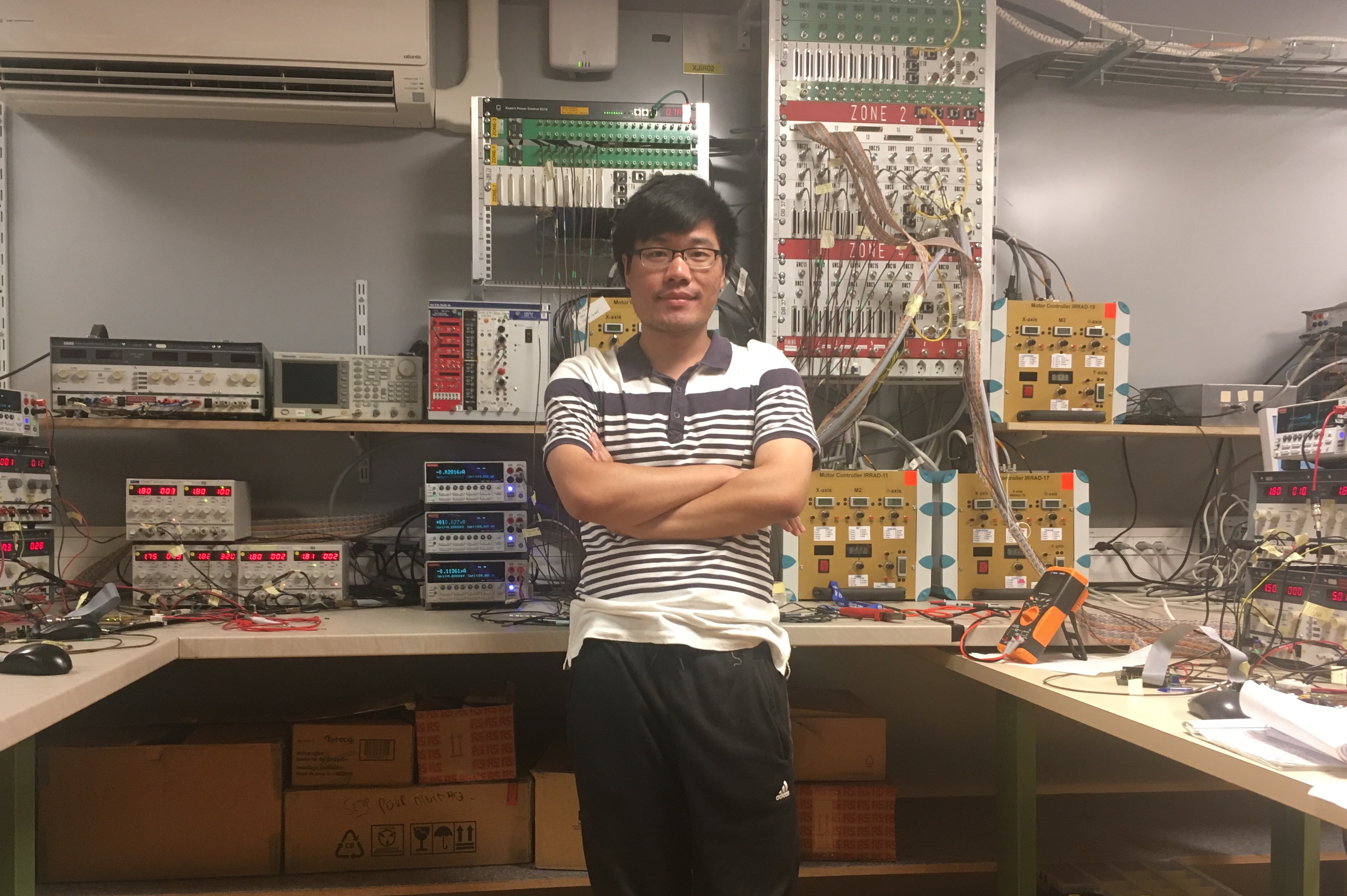
My work covers test setup building, module testing and performance analysis.
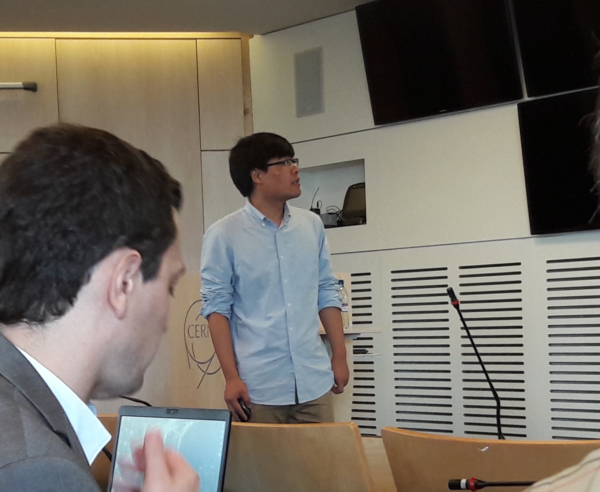
I have already done several secondments to CERN to perform testing at radiation facilities and to work on next generation CMOS design improvement.
|
Host Institution and Secondment Topic |
Expected secondment period |
|
CERN (Geneva, CH), Involvement in irradiation |
4 weeks in August 2018 |
|
Physikalisches Institute Bonn (DE), Test setup common development, Bonn University |
3 weeks in 2018 |
|
CERN (Geneva, CH), Irradiation test |
3 weeks in summer 2018 |
Joining the STREAM ITN is an excellent opportunity for me to continue with studying the area of semiconductor detectors. I am participating in the development of a pixel detector allowing high quality tracking and displaced vertices determination to enhance the reconstruction potential of the upgraded ATLAS detector. These technological opportunities could also have significant impact in critical European sectors such as high energy physics, aerospace, medical Imaging, nano-electronics, etc.
